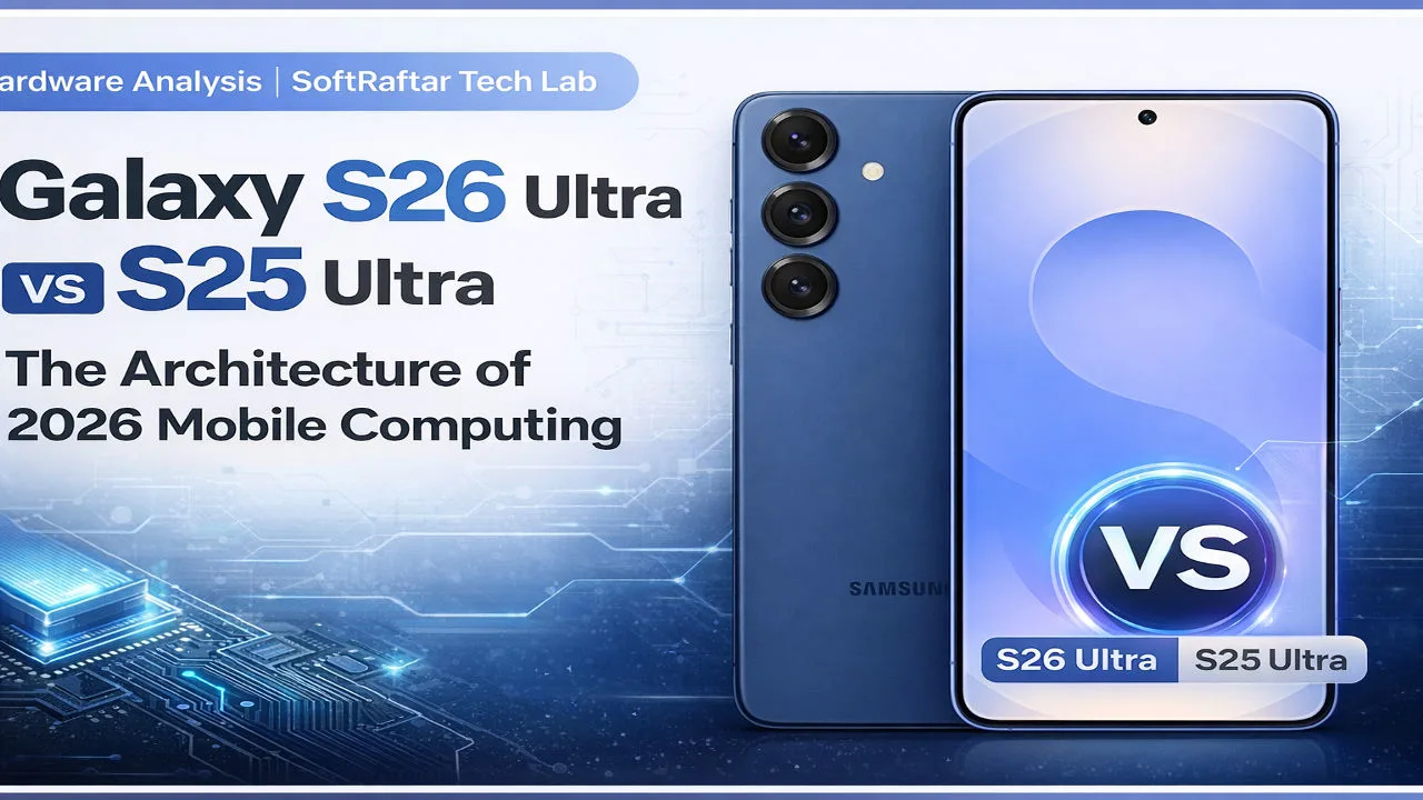
Galaxy S26 Ultra vs S25 Ultra: Next-Gen Mobile Design
Samsung’s 2026 lineup signals a major shift in mobile hardware design
Following Samsung's official February 4th announcements, the technical landscape for mobile enthusiasts has shifted. While the Galaxy S25 Ultra was a high-performance machine for its era, the Galaxy S26 Ultra introduces hardware-level innovations in semiconductor density and optical throughput that resolve long-standing thermal and efficiency bottlenecks.
1. The 2nm Silicon Advantage
These improvements begin at the processor’s manufacturing architecture.
At the heart of the S26 Ultra is the Snapdragon 8 Elite Gen 5. This chipset is built on a 2nm Gate-All-Around (GAA) process, a significant departure from the 3nm architecture found in the Galaxy S25 Ultra. By utilizing GAA transistors, Samsung and Qualcomm have managed to reduce electron leakage, allowing the S26 Ultra to maintain its 4.47 GHz peak frequency for significantly longer durations. For technicians using Termux or heavy software environments, this means stable performance without the sudden frame drops caused by thermal throttling.
2. Technical Specifications Matrix
| Architecture Pillar | Galaxy S25 Ultra (2025) | Galaxy S26 Ultra (2026) |
|---|---|---|
| Manufacturing Node | 3nm FinFET | 2nm GAA (Next-Gen) |
| Primary Aperture | f/1.7 Fixed | f/1.4 (High Intake) |
| Display Material | M13 LTPO | M14 OLED (Power Efficient) |
| Charging Circuit | 45W Single Path | 60W Dual-Cell BMS |
| NPU Throughput | 45 TOPS | 62 TOPS (Real-time AI) |
3. Display Engineering & Efficiency
Samsung’s display gains come from changes at the OLED material level.
The Galaxy S25 Ultra’s screen was rated at 2600 nits using the M13 material set. The S26 Ultra upgrades this to the M14 material set, reaching 3000 nits. However, the real technical win is the Blue-Phosphorescent material. This new organic layer allows the S26 Ultra to achieve higher brightness while consuming 20% less power than the S25 Ultra. This directly impacts "Standby Drain," a common complaint among power users of previous generations.
4. Optics: Photon Capture vs Software Processing
Camera improvements focus on physical optics rather than software correction.
The Galaxy S26 Ultra addresses the physical limitations of the S25 Ultra’s camera. By widening the aperture to f/1.4, the S26 Ultra captures significantly more light (photons) at the hardware level. This reduces the need for the aggressive digital noise reduction seen in S25 Ultra low-light shots, resulting in a 12-bit RAW output that is cleaner and easier to manipulate in post-production software.
60W Charging Logic
The S26 Ultra’s Dual-Cell Battery Management System (BMS) allows for 60W charging without stressing the lithium-ion chemistry, keeping temperatures 15% lower than the S25 Ultra’s 45W cycle.
Thermal Engineering
A new Cryo-Shield Vapor Chamber covers 40% more of the PCB surface, ensuring the 2nm chipset stays within optimal temperature ranges during 8K 30fps recording.
5. Connectivity & Sustained Throughput
Connectivity improvements are driven by changes in antenna architecture
Connectivity has evolved from standard Wi-Fi 7 to Wi-Fi 7+. The S26 Ultra uses a sophisticated antenna array that supports Simultaneous Dual-Band Link on the 6GHz frequency. For users managing remote servers or high-speed data transfers, this architecture reduces latency by 40% compared to the S25 Ultra’s single-link protocol.
SoftRaftar Technical Verdict
The Galaxy S26 Ultra is not just an update; it is a fundamental redesign of mobile hardware. By moving to a 2nm node and a dual-cell charging system, Samsung has solved the primary constraints of the S25 Ultra. For technical users who prioritize sustained performance and imaging precision, the S26 Ultra is the new benchmark for 2026.
SoftRaftar: Engineering the Future of Tech Content.
 Hardware Analysis | SoftRaftar Tech Lab